Our PCBs are superior to those made with conventional adhesion processes:
We are able to create conductors using semi-additive process, starting with down to 1 µm of copper. Guided by the pattern film, these will.
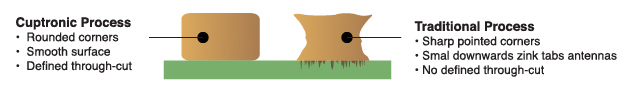
The adhesion surface can be very smooth (Rz<0.1µm) – We are not depending on tabs to adhere the copper, as our process follows the materials inherent topography.
Better Signal Integrity due to improved line definition, shape and resolution. This is the results of minimizing the under etch due to very limited amount of etching and the possibility of smooth surfaces.
Ideally suited for RF and High-Speed applications due to better circuit definition and process consistency between batches.
Ideal for radar manufacture in the automotive, aerospace and defence industries, where high frequencies are required for the detection of 3D objects and objects in motion.
Cuptronic conductors behave more like their theoretical models.
Because of better adhesion and better shaped conductors there will be fewer rejects and less scrapping.
Thinner and straighter connections, leads to fewer layers and holes. Substantial cost reduction due to reduced numbers of layers.
Can be printed on transparent plastic.
For tested PCB materials, please download the PCB presentation.
We are also currently developing a technology for printing lines with laser.
This privacy policy informs you of how Cuptronic Technology AB uses personal information either submitted to us or collected by us online (using cookies).
Cuptronic will always adhere to applicable privacy laws, and will ensure that personal information is handled confidentially. Cuptronic will not, unless bound by law or legally binding decision by an authority, disclose personal information to third parties without prior consent, unless specified specifically herein.
Cuptronic will process the following personal information:
Name, company, email address, and any additional information provided, in order to process at request made by filling out the form on our website www.cuptronic.com.
Your IP address to streamline the use of our website.
If you contact Cuptronic, we will store correspondence or comments, which may contain personal information, to ensure better service if you contact Cuptronic again.
Legality in treatment
Cuptronic will:
Handle your personal information legally, accurately and transparently.
Collect your personal information for the stated and legitimate purposes stated in this policy, and will not process your personal information in any way incompatible with these purposes.
Collect and process personal information that is adequate, relevant and necessary for the purposes for which it is collected and used.
Process your personal information only for as long as necessary for the purposes for which it was collected.
Take appropriate technical and organizational measures to prevent unauthorized access, unlawful processing and unauthorized or accidental loss, destruction or damage to personal information, thereby ensuring an appropriate level of security.
Take all reasonable steps to ensure that your personal information is accurate and updated without delay if Cuptronic is informed or otherwise becomes aware of incorrect information.
If requested, delete personal information without unnecessary delay unless there are legal grounds for continued processing.
If requested, limit processing, unless there are legal grounds for continued processing.
If requested, inform you of the personal data processed by Cuptronic in an accessible and machine-readable form.
Legal basis for processing
Cuptronic collects and processes your personal information if and in so far as you have given consent.
If and in so far as your request results in an agreement between you and Cuptronic, your personal information, collected and processed when the request was made, will be processed to the extent necessary to fulfill Cuptronic’s commitments under the current agreement.
Cuptronic will further process your personal information to the extent that Cuptronic is required to do so by law or decision by an authority.
Personal Data Assistant
Cuptronic allows a Personal Data Assistant to process all personal information through the storage of data and the operation of our systems. The Personal Data Assistant may also read, arrange and send personal information as instructed by Cuptronic.
The Personal Data Assistant only processes your personal information on servers that are within the EU-EEA border and are controlled by the Data Protection Assistant.
Cookies
Cuptronic uses cookies to provide a more user-friendly site. Third-party cookies may also be used (e.g. Google Analytics or other tools) for analytical purposes and/or traffic and visit improvements.
If you do not wish to have cookies installed on your computer, or wish to restrict the processing of such information, your browser may in some cases allow you to opt out or anonymize your IP address.
Security
Cuptronic ensures that appropriate technical and organizational measures are taken to protect your personal information from unauthorized access or destruction, illegal processing or accidental loss or damage.
Cuptronic uses a secure server where your personal data is processed and limits access to personal information within the organization. Authorization to access personal information is provided only to individuals within the organization, as well as to the Personal Data Assistant, for the sole purpose of allowing them to carry out their duties.
Changes to this Privacy Policy
Cuptronic reserves the right to change this privacy policy as required, for example to comply with changes in laws and regulations. Such a change will be published on the Cuptronic website.
Contact
Cuptronic Technology AB
556977-1982
Tallbacksgatan 11 N
195 72 Rosersberg (Stockholm)
Sweden
+46 707 300 000
info@cuptronic.com